
Polyimide Tape for Wave Solder Connector Shielding
Technical Insights · PCB Assembly
Polyimide Tape for Wave Solder Connector Shielding
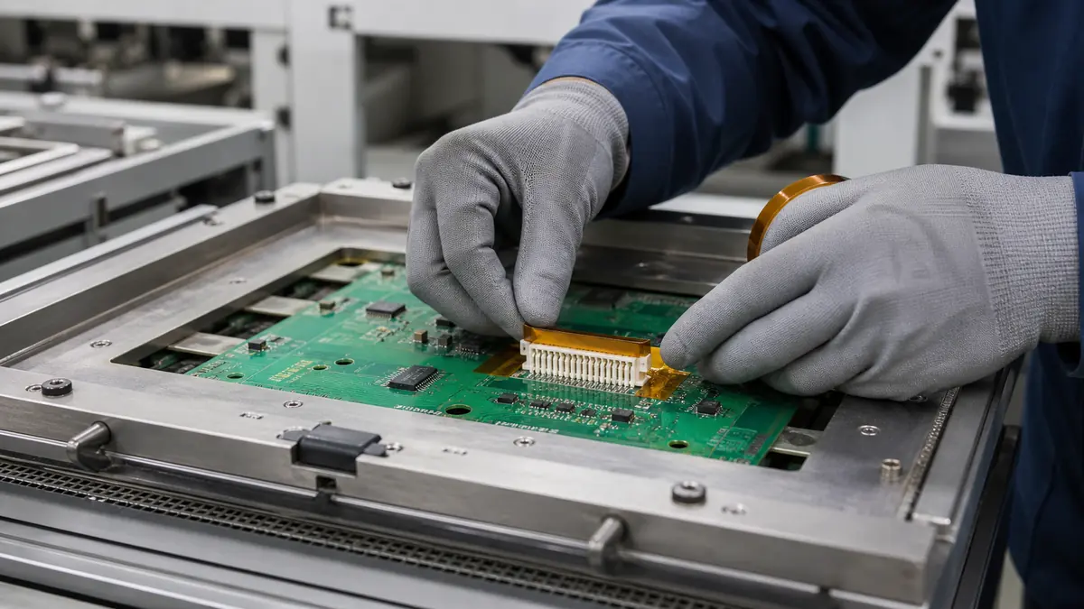
Polyimide tape for wave solder connector shielding can create a temporary, defined barrier around approved connector openings and neighboring PCB features. It must complement the solder pallet, flux control, thermal profile, and inspection plan without covering solderable surfaces or turning an uncontrolled process into an apparently protected one.
Quick Answer
Use polyimide tape only where the released wave-solder process identifies a specific temporary shielding function. Typical candidates include a connector mouth, top-side seam, exposed cavity, or a nearby feature that must remain outside direct flux splash and process debris. The tape does not replace a correctly designed solder pallet, component seating, board support, wave height control, flux setup, preheat profile, nozzle or pot maintenance, and post-solder inspection.
Define the Connector Shielding Role
Wave soldering exposes a populated board to flux, preheat, and a controlled solder contact on the underside. A pallet may support the PCB and expose only the intended solder regions, but some top-side connector geometries still need a temporary local barrier. The approved mask should protect the selected feature without restricting ventilation, trapping contamination, or crossing the solder side.
Separate shielding from unrelated functions. Tape that closes a connector opening may require a different geometry from tape used to retain a loose cover, protect a label, or mark a rework boundary. Each purpose changes the contacted surfaces, peel direction, residue risk, and inspection method.
| Masking location | Possible controlled function | Critical boundary |
|---|---|---|
| Connector opening | Reduce entry of approved process splash or debris | Do not deform contacts, seals, latches, or vents |
| Top-side connector seam | Shield a defined gap near the pallet aperture | Keep adhesive away from mating and inspection surfaces |
| Nearby sensitive feature | Provide a local temporary barrier | Confirm that tape does not redirect heat or contamination |
| Board edge at pallet interface | Close a validated local path | Do not interfere with clamping, grounding, support, or fiducials |
Select the Polyimide Tape Construction
Specify film and adhesive together
Polyimide film supplies a thin, heat-resistant backing, while the adhesive controls initial tack, edge hold, residue, peel force, and interaction with solder mask, connector resin, labels, metals, and pallet surfaces. Approve a traceable construction rather than buying by amber color or a generic “Kapton” description.
Match width and thickness to the geometry
A wide strip is fast to apply but may bridge a connector corner, wrinkle at a change in height, or cover a required inspection zone. A narrower slit width can follow a compact perimeter with less excess build, although more seams increase placement and overlap variation. Use the smallest practical geometry that remains repeatable.
Include flux, cleaner, and ESD controls
Screen the exact flux chemistry, preheat condition, solder exposure, cleaning process, and any electrostatic-control requirement. Tape storage, shelf condition, exposed roll edges, and operator handling can influence contamination and particle control even when the film itself appears unchanged.
| Selection input | What to document | Why it changes the choice |
|---|---|---|
| Tape construction | Film, adhesive, total thickness, width, liner, and lot | Controls handling, adhesion, build, and traceability |
| Contacted materials | Solder mask, connector resin, metal shield, label, and pallet | Each surface can respond differently to heat and peel |
| Solder process | Flux, preheat, solder contact, conveyor, pallet, and cleaning | Defines the real thermal and chemical sequence |
| Mask geometry | Datum, coverage, overlap, keep-outs, and removal tab | Determines repeatability and access |
| Acceptance plan | Solder, residue, connector, electrical, and visual checks | Defines success beyond tape appearance |
Design a Repeatable Masking Boundary
Create a drawing or visual standard that shows the connector, pallet aperture, board reference, tape start and finish points, maximum overlap, and all forbidden zones. Keep adhesive out of connector contacts, latching tracks, sealing surfaces, test points, fiducials, vent paths, solderable pads, plated holes, and areas that must be inspected after soldering.
Square corners can lift when a strip changes direction abruptly. A converted patch with rounded corners, split backing, or a non-adhesive pull tab may improve repeatability when hand-applied strips create too much variation. Any die-cut format still needs tolerance, liner, orientation, packaging, and residue qualification.
Recommended Application Workflow
- Verify revisions. Match PCB, connector, pallet, tape, flux, and work instruction.
- Inspect before masking. Confirm seating, contacts, labels, solder mask, and board cleanliness.
- Prepare controlled pieces. Use the released width and length; keep cut debris away from the assembly.
- Locate the datum. Align to the approved connector or pallet reference without covering fiducials.
- Apply uniform pressure. Seat the tape without flexing the PCB or loading the connector.
- Check all keep-outs. Confirm solderable areas, vents, test points, and clamps remain clear.
- Run the released process. Do not compensate for mask variation by changing wave settings informally.
- Remove and inspect. Peel in the approved direction, count pieces, and examine the complete assembly.
Validate the Complete Wave-Solder Process
Qualification should use representative boards, populated mass, pallet condition, conveyor setup, flux, preheat, solder alloy, wave contact, cooling, and cleaning. Measure the locations identified by the process owner rather than relying only on machine setpoints. Compare the masked connector and neighboring features before and after tape removal.
- Confirm the thermal profile remains within the approved limits for the board and components.
- Inspect solder fill, bridges, icicles, skips, disturbed joints, and flux behavior using the released criteria.
- Check connector contacts, cavities, seals, latches, mating fit, and any required electrical tests.
- Inspect for adhesive residue, lifted solder mask, label damage, loose tape, or transferred particles.
- Requalify changes to tape, connector resin, PCB finish, flux, pallet, profile, cleaning, or mask geometry.
Troubleshooting Common Masking Defects
| Observed problem | Check first | Corrective direction |
|---|---|---|
| Tape edge lifts during preheat | Surface condition, width, corner path, pressure, age, and airflow | Correct the approved geometry and application window |
| Residue remains on connector | Adhesive, resin, heat history, dwell, peel direction, and cleaning | Screen a compatible construction and removal sequence |
| Solder defect appears near mask | Coverage, underside intrusion, pallet aperture, flux, and wave settings | Stop and restore the soldering boundary before release |
| Connector cavity still has debris | Entry path, incomplete seal, wrinkled edge, handling, and removal | Map the actual path and redesign the validated mask |
| Board or component is disturbed on peel | Adhesion, peel angle, support, overlap, and removal temperature | Reduce removal load and improve support under approval |
Related Products and Articles
Frequently Asked Questions
Can polyimide tape replace a wave-solder pallet?
No. A pallet controls board support and solder exposure through designed apertures. Tape may only add the defined temporary local shield in a qualified process.
Should tape cover the connector pins?
Not unless the released drawing specifically defines that contact and subsequent inspection. Adhesive must not contaminate mating, soldering, sealing, or electrical surfaces.
Does amber color prove suitability for wave soldering?
No. Color does not identify film thickness, adhesive chemistry, residue behavior, or process compatibility. Approve the exact tape construction.
Is one wide strip better than several narrow strips?
It depends on connector geometry, keep-outs, corner conformity, overlap, access, and cycle time. Compare both layouts on the real board and pallet.
What information belongs in an RFQ?
Provide the PCB and connector drawings, pallet aperture, masking function, contacted materials, flux and solder process, cleaning, dimensions, quantity, and validation plan.
Build a Controlled Wave-Solder Masking Trial
Share the connector and PCB geometry, pallet interface, keep-out drawing, current tape format, flux, preheat and solder sequence, cleaning process, production volume, and acceptance tests. JIAO TAO TAO can help shortlist polyimide tape constructions and converted formats for process qualification.
Discuss connector shieldingPTFE Tape for Thermoforming Heater Plate Release Surfaces
PTFE Tape for Shrink-Wrap L-Sealer Release Surfaces
Related Article

Need help choosing the right industrial tape?
Send us your application details, including temperature, surface material, size, quantity and current problem. Our team will help recommend a suitable tape material or custom die-cut solution.

simon@jiaotaotao.com


+86-136 1277 5969


+86-136 1277 5969
