
Wave Soldering Tape 280°C: PET Silicone Guide & Specs
Wave Soldering Tape: Technical Guide for PCB Gold Finger & THT Connector Protection
By Jiaotaotao Product Department - Xindy | Updated: 2026 | View Product Range →
JIAOTAOTAO Tape manufacturer — Dongguan Factory Direct
What Is Wave Soldering Tape?
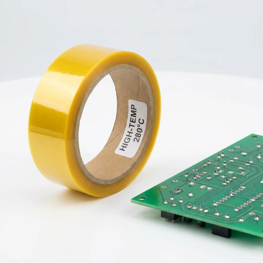
Wave soldering tape is a high-temperature pressure-sensitive adhesive tape constructed with a biaxially oriented polyester (PET) film backing coated with a cross-linked silicone adhesive system, applied to printed circuit boards immediately before the wave soldering process to protect designated areas—gold-plated edge connectors, through-hole (THT) connector bodies, test pads, and pre-installed SMT components—from direct contact with molten solder at 245–260°C. It is engineered to maintain edge-seal integrity and zero adhesive transfer through the full wave soldering thermal cycle, then remove cleanly without contaminating gold-plated or soldermask surfaces. Operating peak rating: 280°C short-term; continuous service: 200°C.
Quick Facts
- Backing material: Biaxially oriented PET film (BoPET), 36–50 µm
- Adhesive system: Cross-linked silicone PSA
- Continuous service temperature: 200°C
- Short-term peak (wave soldering): 280°C
- Dielectric strength: ≥ 5,000 V (per ASTM D1000)
- Residue-free removal: Zero adhesive transfer after SAC305 wave solder cycle confirmed
- Core uses: Gold finger protection, THT connector masking, selective soldering, SMT reflow, conformal coating dam
- Colors available: 13+ standard colors for process-line color-coding
- Manufacturer: JIAOTAOTAO Tape manufacturer, Dongguan, China (Est. 2009)
Technical Specifications & Material Science
Why PET Film Outperforms Paper Backing in Wave Soldering
Traditional paper-backed masking tapes absorb flux activators and moisture during the wave soldering preheat zone (100–150°C), causing the paper to soften and the tape edge to lift. A lifted edge allows solder to wick beneath the tape and contaminate gold-plated contacts—a defect classified as a Class 3 workmanship violation under IPC-A-610. BoPET film does not absorb flux or moisture, maintains its dimensional form through preheat and solder contact, and provides thermal shrinkage <1.5% at 150°C for 30 minutes (ASTM D1504), keeping the tape edge pressed flat against the PCB soldermask surface throughout the full thermal cycle.
Silicone Adhesive: Performance at 280°C Wave Contact
The silicone adhesive system is a thermally cross-linked polydimethylsiloxane (PDMS) network. The Si–O backbone bond energy (~450 kJ/mol) is significantly higher than C–C (~346 kJ/mol) or C–O (~360 kJ/mol) bonds in acrylic systems. This structural advantage enables the adhesive to survive 280°C molten solder contact for 3–8 seconds without chain scission or adhesive mass transfer. After the solder wave passes, the adhesive cools and can be peeled cleanly—no solvent wiping, no mechanical abrasion, no contact resistance increase on gold fingers.
Standard Technical Parameters — JIAOTAOTAO Tape PET Silicone Wave Soldering Tape
| Parameter | Value | Test Standard |
|---|---|---|
| Total Tape Thickness | 0.055 mm (55 µm) ± 5% | ASTM D1000 |
| PET Backing Thickness | 36 µm | ASTM D374 |
| Adhesive Type | Cross-linked silicone PSA | — |
| Adhesive Thickness | 19 µm ± 2 µm | ASTM D1000 |
| Continuous Service Temperature | 200°C | IEC 60454-2 |
| Short-Term Peak Temperature | 280°C (wave solder contact, ≤10 sec) | IEC 60454-2 |
| Tensile Strength | ≥ 150 N/25 mm | ASTM D1000 |
| Elongation at Break | ≥ 80% | ASTM D1000 |
| Dielectric Strength | ≥ 5,000 V | UL 510 / ASTM D149 |
| Adhesion to Steel (180° Peel) | ≥ 8 N/25 mm | PSTC-101 |
| Thermal Shrinkage (150°C / 30 min) | < 1.5% | ASTM D1504 |
| Edge Bleed (255°C / wave contact) | < 0.1 mm | Internal method |
| Flux Resistance | IPA, acetone, RMA / RA rosin flux, no-clean flux (J-STD-004) | — |
| Flame Retardancy (film) | UL94 V-0 | UL 94 |
| Available Width Range | 3 mm – 1,200 mm (custom slit) | — |
| Standard Colors | 13+ (amber, yellow, blue, red, green, black, transparent, pink, orange, purple, rose red, deep yellow, white) | — |
| Shelf Life | 24 months (5–30°C, RH ≤ 65%) | — |
Wave Soldering Process Applications
1. Gold Finger & Edge Connector Protection During Wave Soldering
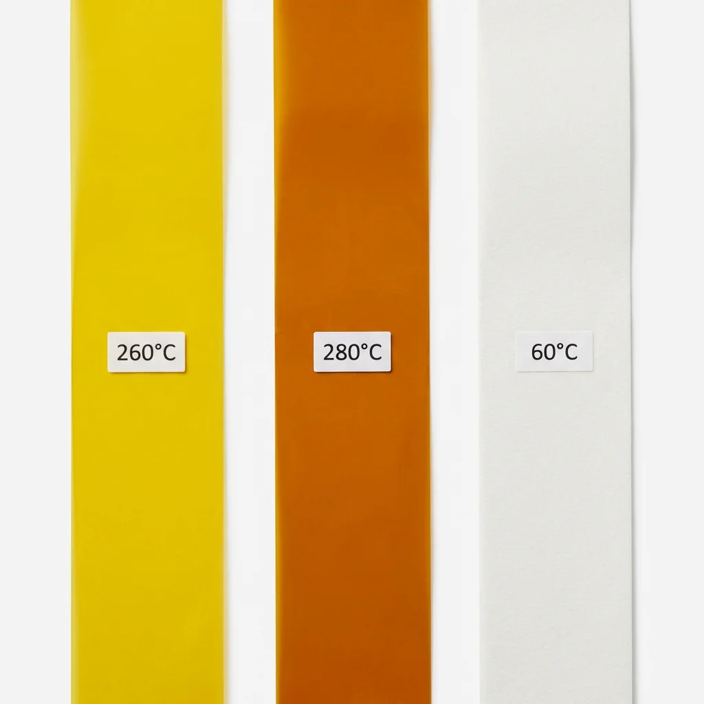
Gold-plated edge connectors (ENIG or hard gold per IPC-4552) on PCIe, DDR, and industrial I/O boards are positioned at the board edge directly above the wave solder bath. Solder alloy temperatures for SAC305 lead-free process range from 250–260°C with 3–8 seconds contact time. Any tape-edge lift during this contact exposes the gold surface to solder bridging, flux contamination, and intermetallic compound formation—all of which degrade contact resistance above the IPC-4552 maximum of 10 mΩ. JIAOTAOTAO Tape's PET silicone wave soldering tape maintains edge bleed <0.1 mm at 255°C, completely enclosing the gold contact area throughout the solder pass.
2. THT Connector & Component Body Masking
Through-hole (THT) connectors—USB, RJ45, power jacks, D-sub—have plastic housings rated to 85–105°C. Direct wave solder contact at 255°C melts or deforms these housings. Wave soldering tape wrapped around or applied over the connector body reflects heat and blocks direct solder contact, preserving dimensional accuracy of connector alignment pins and locking tabs. The tape's PET backing acts as a thermal barrier; its silicone adhesive holds position under the turbulence of the solder wave without displacement.
3. Mixed SMT / THT Board — Pre-Populated Component Protection
Mixed-technology boards with SMT components on the bottom side pass through the wave upside-down, exposing pre-populated capacitors, IC packages, and connectors to direct solder contact. Components outside the wave solder target zones are masked with tape prior to machine entry. Tape conformability (elongation ≥80%) is critical for wrapping around component bodies and lead exits without leaving gaps at component edges. PET film's flexibility allows coverage of irregular surface profiles without tearing.
4. Selective Soldering — Precision Adjacent-Area Masking
Selective soldering nozzles reach 260–280°C and target individual THT pins within 1–3 mm of adjacent SMT components. Narrow-slit wave soldering tape (3–10 mm widths) provides precision edge masking of adjacent fine-pitch connectors and test pads. The tape's resistance to rosin-based flux activators prevents flux wicking beneath the tape edge—a defect that causes soldermask discoloration visible under IPC-A-610 automated optical inspection (AOI).
5. Post-Solder ICT Test Pad Preservation
In-circuit test (ICT) fixtures probe bare copper or HASL test pads. Flux residue and solder splash during wave soldering can contaminate these pads, raising contact resistance above the 50 mΩ ICT maximum and triggering false failures. Masking ICT pads during wave soldering preserves pad surface cleanliness without requiring post-process chemical cleaning steps, reducing cycle time on high-volume assembly lines.
PET Silicone vs Polyimide vs Paper: How to Select Wave Soldering Tape
Three tape constructions are used in wave soldering masking. The comparison below addresses process qualification criteria for SAC305 lead-free wave soldering at 250–260°C.
| Parameter | PET + Silicone (JIAOTAOTAO Tape, 280°C) |
Polyimide (Kapton) + Silicone |
Paper + Rubber / Acrylic |
|---|---|---|---|
| Short-Term Peak Temp | 280°C ✓ | 300°C+ ✓ | 120°C ✗ |
| Wave Soldering Qualified | ✓ Yes | ✓ Yes | ✗ No |
| Residue-Free Removal | ✓ Confirmed | ✓ Confirmed | ✗ Carbonized residue |
| Flux / Moisture Absorption | None (PET film) | None | High (paper absorbs flux) |
| Edge Lift Risk at 255°C | None ✓ | None ✓ | High ✗ |
| Dielectric Strength | ≥ 5,000 V | ≥ 7,000 V | < 1,000 V |
| Cost vs Performance | Optimal ✓ | High cost (3–5×) | Low cost, process failure risk |
| Color Options | 13+ colors | Amber only | Beige / white only |
| Width Availability | 3–1,200 mm | 3–610 mm (typical) | 6–150 mm (typical) |
Selection rule: For SAC305 wave soldering at 250–260°C, PET silicone tape is the qualified standard specification at optimal cost. Paper-backed tapes are not qualified for any lead-free wave soldering process and should be eliminated from the approved materials list. Polyimide tape provides a 20°C additional thermal margin but at 3–5× cost premium—justified only for selective soldering nozzle temperatures exceeding 280°C or for permanent board-level insulation applications.
Customization & Supply Capabilities
JIAOTAOTAO Tape manufacturer is established in Dongguan, Guangdong (2009), operating 8 automated coating lines across a 6,000 m² production facility. Certifications: ISO 9001:2015 · SGS · UL94 V-0. All products supplied direct from factory — no distributor margin.
- Custom Width Slitting: 3 mm to 1,200 mm in 0.5 mm increments, ±0.5 mm tolerance. Narrow widths (3–15 mm) standard for selective soldering and gold finger masking.
- Die-Cut Masking Pads: Custom footprints for specific connector outlines (USB-A/B/C, RJ45, D-sub, PCIe x1/x4/x16). Tolerance ±0.2 mm. Kiss-cut on liner for peel-and-place production use.
- Roll Arrays: Multiple pad widths gang-cut on a single liner — one peel covers multiple masking zones simultaneously, reducing application cycle time on high-volume SMT lines.
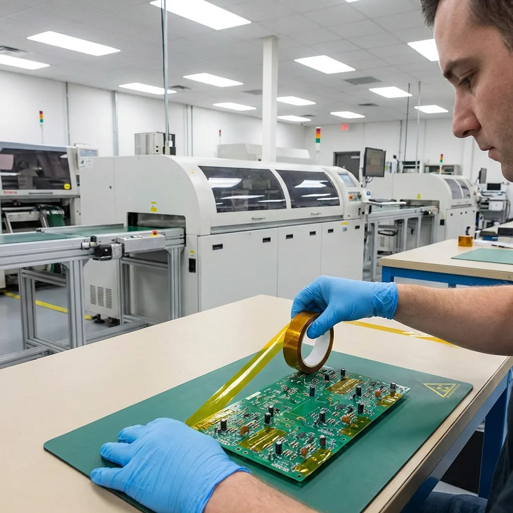
- Process Color-Coding: 13+ standard colors enable visual differentiation across process stages (e.g., yellow = wave solder zone, blue = conformal coating zone, red = do-not-solder marker).
- Custom Roll Length: Standard 33 m; OEM options at 50 m / 100 m. Core ID: 25 / 50 / 76 mm.
- Private Label / OEM Packaging: Core printing, carton labeling, and co-branded packaging for EMS and distributor programs.
- Free Qualification Samples: 1–3 widths dispatched within 5 business days. Specify solder alloy (SAC305 / SnPb), bath temperature, and gold finger pitch for adhesive weight recommendation.
- MOQ: 1 carton (~20–50 rolls for standard widths). Die-cut tooling: one-time setup fee, no per-run MOQ premium.
- Lead Time: Standard slit widths: 7–15 business days ex-factory. Custom die-cut: 15–25 business days.
FAQ for PCB Engineers & Procurement

Q1: What temperature does wave soldering tape need to withstand, and does PET silicone tape qualify?
SAC305 lead-free wave soldering operates at 250–260°C bath temperature with 3–8 seconds PCB contact time per IPC-A-610 process guidelines. JIAOTAOTAO Tape PET silicone wave soldering tape is rated to 280°C short-term, providing a 20–30°C thermal margin above the process requirement. The tape has been process-qualified against SAC305 at 255°C for 8-second contact duration with zero edge lift or adhesive transfer recorded. SnPb eutectic processes (183°C bath) present no thermal challenge for this tape.
Q2: Will wave soldering tape leave residue on gold fingers or PCB soldermask after removal?
Zero residue is confirmed by 180° peel testing on ENIG gold-finished test coupons post-255°C wave solder cycle per PSTC-101. The cross-linked silicone adhesive network retains full cohesive strength through thermal cycling—no adhesive mass is transferred to the gold surface. Gold finger contact resistance post-removal measures within IPC-4552 specification (<10 mΩ) without cleaning. Paper-backed tapes and acrylic-adhesive PET tapes carbonize above 150°C, leaving deposits that raise contact resistance and require IPA wipe-down or mechanical abrasion.
Q3: When is the correct time to remove wave soldering tape after the solder bath?
Remove tape within 30–60 seconds of board exit from the wave soldering machine, while board temperature is still above 50°C. At this temperature, silicone adhesive peel force is 6–10 N/25 mm—its minimum. As the board cools to room temperature, the adhesive re-anchors to the substrate, increasing peel force by 30–50% and risking soldermask micro-delamination at tape edges adjacent to fine-pitch component pads. Establish a process SOP specifying removal within 60 seconds, enforced at the unload station immediately after the cooling conveyor.
Q4: Can the same tape be used for both wave soldering masking and conformal coating masking on the same board?
Yes. The same PET silicone tape qualifies for both process stages. For conformal coating, the tape provides a void-free coating dam against acrylic, polyurethane, silicone, and epoxy coatings per IPC-CC-830. Apply fresh tape after wave soldering and before conformal coat—do not reuse the wave solder tape for the coating stage, as the adhesive surface may have accumulated flux chemistry that reduces adhesion to the PCB soldermask. Using color-coded tape by process stage (yellow for wave solder, blue for conformal coat) eliminates this error in production.
Q5: What width should be ordered for gold finger masking, and is custom die-cutting available?
Width = gold finger contact zone length + 3 mm overlap on each side onto PCB soldermask. For PCIe x16 gold fingers (67.7 mm contact length), specify 73–75 mm width tape. For DDR4 DIMM (85 mm contact zone), specify 91–92 mm. Custom die-cut pads matching exact connector outlines—including notches for alignment tabs—are available at ±0.2 mm tolerance, kiss-cut on liner. Specify connector type, contact count, and PCB edge thickness when requesting die tooling quotes from JIAOTAOTAO Tape manufacturer.
Q6: How does wave soldering tape interact with no-clean flux and aqueous wash cleaning systems?
The silicone adhesive and PET film are inert to no-clean flux activators (organic acid and rosin chemistries, J-STD-004 ORL0/ORM0 classifications). In aqueous wash systems (saponifier 5–10% concentration, 40–60°C, spray pressure 20–30 PSI), the tape maintains adhesion through wash and rinse stages. For extended soak in alkaline saponifiers above pH 11 exceeding 30 minutes, pre-qualify adhesion retention on the specific board soldermask chemistry. Tape should be removed before solvent cleaning with ketones (MEK, acetone) as these may soften the silicone adhesive boundary.
Q7: How does JIAOTAOTAO Tape compare to 3M 1280, Nitto 923S, and Kapton tape for wave soldering?
3M 1280 and Nitto 923S are PET/silicone constructions with 260–280°C wave soldering ratings and 55–65 µm total thickness—specifications equivalent to JIAOTAOTAO Tape's silicone series. Kapton (polyimide) tape provides 300°C+ rating at 3–5× cost premium with no performance advantage for standard SAC305 wave soldering at 255°C. JIAOTAOTAO Tape matches 3M/Nitto performance specifications at direct-factory pricing, eliminating 30–60% distributor margin, with 13+ color options and full OEM die-cut capability unavailable from brand-name distributors.
Request a Data Sheet, Free Sample, or Factory Quote
JIAOTAOTAO Tape manufacturer PET silicone wave soldering tape — 280°C short-term peak · zero adhesive residue · ≥5,000 V dielectric · UL94 V-0 · 13+ colors — covers all SAC305 and SnPb wave soldering, selective soldering, SMT reflow masking, conformal coating, and ICT pad protection requirements. Available in standard slit widths from 3 mm, custom die-cut connector pads, and OEM/private label formats. Direct from Dongguan factory.
Contact JIAOTAOTAO Tape Manufacturer Directly:
- 📋 Request TDS / Process Qualification Report: simon@jiaotaotao.com
- 🧪 Free Sample: State solder alloy type, bath temp, gold finger pitch & connector type — dispatched within 5 business days
- 💬 WhatsApp / WeChat: +86-136 1277 5969
- 🔗 Full Polyester Tape Range: www.clothadhesive.com/polyester-tape.html
- 📝 Online Inquiry: Send Inquiry →
Powder Coating Masking Tape 200°C: PET Silicone Green Guide
PCB Masking Tape 280°C: PET Silicone Guide for Wave Soldering
Related Article
Need help choosing the right industrial tape?
Send us your application details, including temperature, surface material, size, quantity and current problem. Our team will help recommend a suitable tape material or custom die-cut solution.

simon@jiaotaotao.com


+86-136 1277 5969


+86-136 1277 5969
