
Gold Finger Masking Tape: Polyimide Guide for PCB Edge Connector Protection
Gold Finger Masking Tape: Technical Guide for PCB Edge Connector & ENIG Surface Protection
By Jiaotaotao Product Department - Xindy | Updated: 2026 | View Product Range →
JIAOTAOTAO Tape manufacturer — Dongguan Factory Direct
What Is Gold Finger Masking Tape?
Gold finger masking tape is a high-temperature pressure-sensitive adhesive tape constructed with a polyimide (PI) film backing coated with a cross-linked silicone adhesive system, applied to PCB gold-plated edge connectors—commonly called "gold fingers"—before SMT reflow, wave soldering, selective soldering, conformal coating, and electroplating processes. It protects the gold-plated contact surface from solder bridging, flux contamination, intermetallic compound (IMC) formation, and coating overspray, then removes cleanly without adhesive transfer onto the ENIG or hard gold surface. Operating peak rating: 300°C short-term; continuous service: 260°C. The amber-colored polyimide film is the industry-recognized standard for gold finger protection in IPC-A-610 Class 2 and Class 3 PCB assembly.
Quick Facts
- Backing material: Polyimide (PI) film — DuPont Kapton equivalent, 25–50 µm
- Adhesive system: Cross-linked silicone PSA
- Continuous service temperature: 260°C
- Short-term peak (reflow / wave contact): 300°C
- Dielectric strength: ≥ 7,000 V (per ASTM D149)
- Residue-free removal: Zero adhesive transfer on ENIG and hard gold contacts confirmed post-SAC305 reflow and wave solder cycle
- Contact resistance post-removal: < 10 mΩ per IPC-4552 specification
- Core uses: Gold finger edge connector protection, ENIG pad masking, electroplating selective masking, conformal coating dam, ICT test pad preservation
- Standard color: Amber (polyimide film natural color)
- Manufacturer: JIAOTAOTAO Tape manufacturer, Dongguan, China (Est. 2009)

Technical Specifications & Material Science
Why Polyimide Film Is the Preferred Backing for Gold Finger Masking
Polyimide film (tradename Kapton, DuPont) is synthesized through condensation polymerization of pyromellitic dianhydride (PMDA) and 4,4'-oxydianiline (ODA), producing an aromatic imide ring structure with exceptional thermal stability. The glass transition temperature (Tg) of polyimide film exceeds 400°C, compared to 70–80°C for PET film and <200°C for paper. This structural advantage allows the polyimide backing to survive 260°C continuous service and 300°C short-term peak during lead-free SAC305 reflow profiles without dimensional deformation, edge lifting, or carbonization. The film's thermal shrinkage is <0.3% at 200°C / 30 minutes—five times better than PET film—maintaining edge-seal integrity across multi-pass reflow profiles where boards traverse 2–4 oven passes.
Silicone Adhesive: Zero Residue on Gold Contact Surfaces
The silicone PSA is a thermally cross-linked polydimethylsiloxane (PDMS) network. Unlike acrylic adhesives that undergo oxidative chain scission above 150°C—depositing carbonized adhesive residue on gold surfaces that raises contact resistance above IPC-4552's 10 mΩ limit—the silicone network retains full cohesive integrity through 300°C peak reflow and 260°C wave solder contact. Post-removal contact resistance on ENIG gold surfaces measures <5 mΩ without cleaning, confirming zero ionic contamination or adhesive mass transfer onto the gold contact area. This is critical for gold finger edge connectors interfacing with PCIe, DDR, M.2, and industrial backplane slots rated to Class 3 workmanship per IPC-A-610.
Standard Technical Parameters — JIAOTAOTAO Tape Polyimide Gold Finger Masking Tape
| Parameter | Value | Test Standard |
|---|---|---|
| Total Tape Thickness | 0.065 mm (65 µm) ± 5% | ASTM D1000 |
| Polyimide Film Thickness | 25 µm / 50 µm (two grades available) | ASTM D374 |
| Adhesive Type | Cross-linked silicone PSA | — |
| Adhesive Thickness | 38 µm ± 3 µm | ASTM D1000 |
| Continuous Service Temperature | 260°C | IEC 60454-2 |
| Short-Term Peak Temperature | 300°C (reflow peak / wave contact, ≤10 sec) | IEC 60454-2 |
| Tensile Strength | ≥ 200 N/25 mm | ASTM D1000 |
| Elongation at Break | ≥ 70% | ASTM D1000 |
| Dielectric Strength | ≥ 7,000 V | ASTM D149 / UL 510 |
| Adhesion to Steel (180° Peel) | ≥ 10 N/25 mm | PSTC-101 |
| Contact Resistance Post-Removal (ENIG) | < 10 mΩ (IPC-4552 compliant) | IPC-4552 |
| Thermal Shrinkage (200°C / 30 min) | < 0.3% | ASTM D1504 |
| Edge Bleed (260°C / wave contact) | < 0.1 mm | Internal method |
| Flux Resistance | IPA, rosin (RMA/RA), no-clean flux (J-STD-004 ORL0/ORM0), water-soluble flux | — |
| Flame Retardancy (film) | UL94 V-0 | UL 94 |
| Available Width Range | 2 mm – 620 mm (custom slit) | — |
| Shelf Life | 24 months (5–30°C, RH ≤ 65%) | — |
PCB Assembly Process Applications
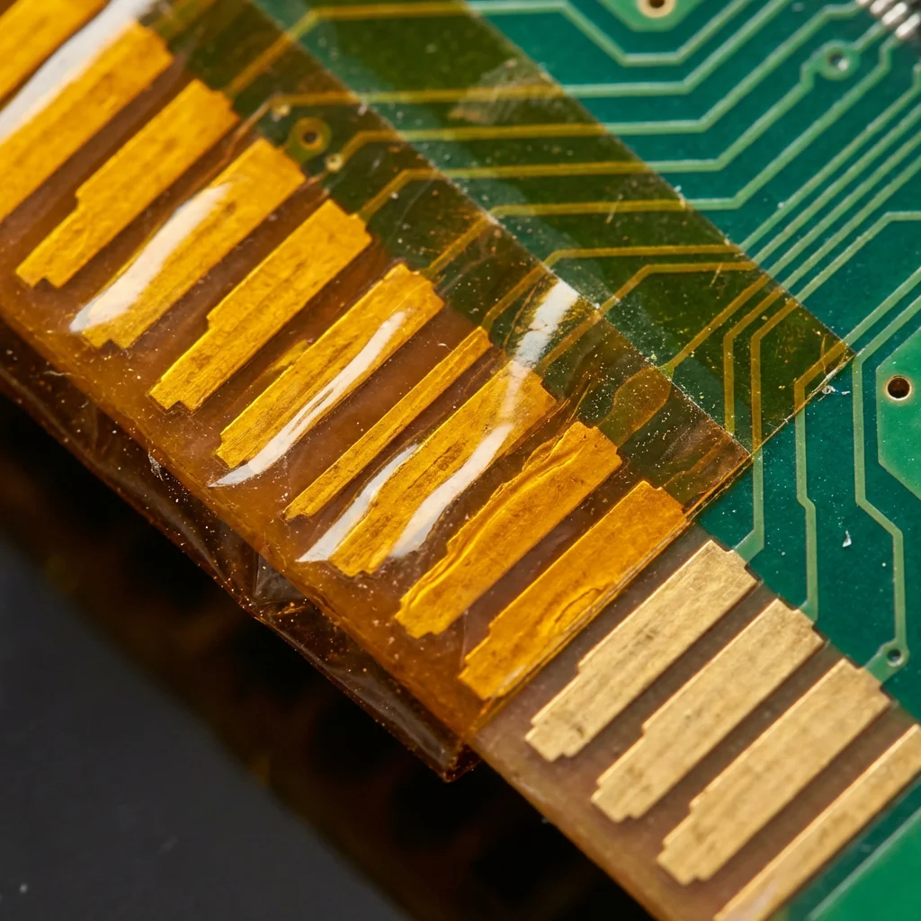
1. SMT Reflow Oven — Gold Finger Protection Across Multi-Pass Profiles
Lead-free SAC305 SMT reflow profiles reach peak zone temperatures of 245–260°C, with boards spending 30–60 seconds above liquidus (217°C) per J-STD-020 qualification. Double-sided boards traverse the reflow oven twice—exposing gold finger edge connectors to cumulative thermal stress across two complete reflow profiles. Polyimide film's Tg >400°C and thermal shrinkage <0.3% at 200°C ensures the tape remains flat and fully adhered across both oven passes without repositioning. PET-backed tape (Tg ~70°C) cannot be used for multi-pass reflow applications—it softens and lifts during the first pass, exposing the gold finger area to flux fumes and reflow atmosphere oxidation that discolors the gold surface.
2. Wave Soldering — Edge Connector Solder Bridge Prevention
Wave soldering bath temperatures for SAC305 range from 250–260°C with 3–8 seconds contact time. Gold finger contacts positioned at the PCB board edge pass directly above the solder wave. Without masking, molten solder wicks onto gold finger contacts by capillary action, forming solder bridges between adjacent contacts. On fine-pitch gold fingers (0.5 mm–1.0 mm pitch), a single bridge causes a Class 3 defect under IPC-A-610 that requires manual rework with micro-soldering irons. JIAOTAOTAO Tape polyimide masking tape maintains edge bleed <0.1 mm at 260°C, completely enclosing the gold contact zone throughout the solder pass with zero solder infiltration.
3. Selective Electroplating — Hard Gold Thickness Masking
Gold finger contacts on high-cycle-life connectors (PCIe, DDR, industrial backplane) receive hard gold (Co-Au alloy) plating at 0.76–1.27 µm thickness per IPC-4552A, while the remaining board surface receives ENIG or HASL finish at lower cost. The electroplating mask must survive the plating bath chemistry (gold sulfite or gold cyanide at pH 6–9, 50–65°C) without delamination or electrolyte infiltration beneath the tape edge. Polyimide film is chemically inert to gold plating bath chemistry; the silicone adhesive provides electrolyte-resistant sealing at the tape boundary, preventing plating solution from reaching unmasked areas and causing unwanted gold deposition.
4. Conformal Coating — Gold Contact Zone Exclusion
Conformal coating (acrylic, polyurethane, silicone, or epoxy per IPC-CC-830) applied over gold finger contacts causes contact resistance to increase above the 50 mΩ IPC-A-610 maximum for edge connector interfaces. Coating penetration into the connector slot also prevents physical card insertion. Polyimide masking tape applied to the gold finger area before conformal coat spray provides a void-free coating dam with <0.1 mm edge boundary accuracy, preventing overspray onto gold contacts. The tape is removed post-coating while the coating is still slightly tacky (within 15 minutes of spray) to achieve a clean, straight coating boundary.
5. ICT & Functional Test Pad Preservation
In-circuit test (ICT) fixtures probe ENIG or HASL test pads adjacent to the gold finger area. Flux residue, solder splash, and conformal coating overspray from upstream processes can contaminate test pads, raising contact resistance above the 50 mΩ ICT probe contact maximum and causing false failures on production test. Masking critical test pads with polyimide tape during soldering and coating processes preserves pad cleanliness without requiring post-process solvent cleaning, reducing cycle time and eliminating IPA solvent handling on high-volume SMT lines.
Polyimide vs PET Silicone vs Paper: How to Select Gold Finger Masking Tape
Three tape backing materials are used in gold finger masking applications. The selection matrix below addresses IPC-A-610 Class 3 process requirements for SAC305 reflow and wave soldering at 245–260°C.
| Parameter | Polyimide + Silicone (JIAOTAOTAO, 300°C) |
PET + Silicone (280°C) |
Paper + Rubber / Acrylic |
|---|---|---|---|
| Short-Term Peak Temp | 300°C ✓ | 280°C ✓ | 120°C ✗ |
| Multi-Pass Reflow Qualified | ✓ Yes (4+ passes) | ✓ 1–2 passes only | ✗ No |
| Thermal Shrinkage at 200°C | <0.3% ✓ | <1.5% | Deforms / carbonizes |
| ENIG Residue-Free Removal | ✓ <5 mΩ | ✓ <10 mΩ | ✗ Carbonized deposits |
| Edge Bleed at 260°C | <0.1 mm ✓ | <0.1 mm ✓ | Edge lift, uncontrolled |
| Dielectric Strength | ≥ 7,000 V | ≥ 5,000 V | <1,000 V |
| Electroplating Bath Resistance | ✓ Full resistance | ✓ Partial | ✗ Absorbs electrolyte |
| IPC-A-610 Class 3 Qualified | ✓ Yes | ✓ Class 2 | ✗ Not qualified |
| Cost vs Performance | Optimal for Class 3 ✓ | Lower cost, Class 2 use | Lowest cost, unqualified |
Selection rule: For IPC-A-610 Class 3 gold finger protection through SAC305 reflow (245–260°C) and wave soldering (250–260°C), polyimide silicone tape is the required specification. PET silicone tape qualifies for Class 2 single-pass applications where peak temperatures do not exceed 260°C. Paper-backed tapes are disqualified for all lead-free soldering processes and must be removed from approved materials lists for gold finger masking.

Customization & Supply Capabilities
JIAOTAOTAO Tape manufacturer is established in Dongguan, Guangdong (2009), operating 8 automated coating lines across a 6,000 m² production facility. Certifications: ISO 9001:2015 · SGS · UL94 V-0. All polyimide tape products supplied direct from factory — no distributor margin.
- Custom Width Slitting: 2 mm to 620 mm in 0.5 mm increments, ±0.5 mm tolerance. Precision narrow widths (2–15 mm) for fine-pitch gold finger masking; wide rolls (50–200 mm) for full edge-connector zone coverage.
- Gold Finger Width Calculation Service: Specify connector type (PCIe x1/x4/x8/x16, DDR4/DDR5, M.2, DIMM, industrial backplane pitch), contact count, and board edge thickness — JIAOTAOTAO Tape engineers calculate the correct tape width with 3 mm soldermask overlap recommendation.
- Die-Cut Connector Pads: Custom-profile die-cut pads matching exact gold finger zone outlines, including notches for alignment tabs and keying slots. Kiss-cut on liner for peel-and-place production use. Tolerance ±0.2 mm.
- PI Film Thickness Options: 25 µm film for fine-pitch connectors where tape-edge step height is critical to board slot clearance; 50 µm film for standard gold finger masking with higher tear resistance during manual application.
- Double-Sided Polyimide Tape: Available for component fixturing, flex circuit lamination, and transformer insulation layer applications — specify application on inquiry.
- Custom Roll Length: Standard 33 m; OEM options at 50 m / 100 m. Core ID: 25 / 50 / 76 mm.
- Free Qualification Samples: 1–3 widths dispatched within 5 business days. Specify connector type, gold finish (ENIG / hard gold / OSP), reflow profile peak temperature, and number of oven passes for adhesive weight recommendation.
- MOQ: 1 carton (~20–50 rolls for standard widths). Die-cut tooling: one-time setup fee, no per-run MOQ premium after tooling approval.
- Lead Time: Standard slit widths: 7–15 business days ex-factory. Custom die-cut pads: 15–25 business days including tooling fabrication.
FAQ for PCB Engineers & Procurement
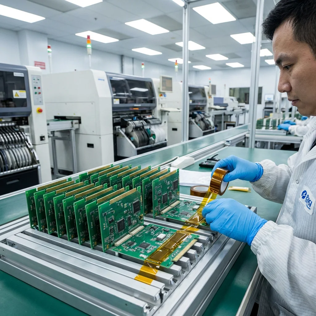
Q1: Why is polyimide tape specifically required for gold finger masking rather than standard PET tape?
Polyimide film has a glass transition temperature (Tg) exceeding 400°C, compared to 70–80°C for PET film. On double-sided PCBs passing through two reflow oven cycles at 245–260°C, PET-backed tape softens and lifts during the first pass, exposing gold fingers to flux fume oxidation and reflow atmosphere contamination that permanently discolors the gold surface. Polyimide tape maintains dimensional stability across 4+ reflow passes, making it the mandatory specification for IPC-A-610 Class 3 assemblies including server boards, industrial control systems, and telecommunications equipment.
Q2: What contact resistance increase should be expected on gold fingers after tape removal?
Zero measurable contact resistance increase is observed when using polyimide silicone tape on ENIG gold surfaces. Post-removal measurement on ENIG test coupons after SAC305 wave solder cycle records <5 mΩ—well within IPC-4552A's 10 mΩ maximum for gold edge connector contacts. This compares to 15–50 mΩ increase observed after paper-backed acrylic tape removal post-200°C bake, where carbonized adhesive residue requires IPA cleaning before the surface returns to specification. No cleaning step is required after JIAOTAOTAO Tape polyimide tape removal.
Q3: What is the correct tape width for masking PCIe, DDR4, DDR5, and M.2 gold finger contacts?
Tape width = gold finger contact zone length + 3 mm soldermask overlap on each side. Standard connector specifications: PCIe x16 contact zone = 67.7 mm → use 73–75 mm tape. DDR4 DIMM contact zone = 85.0 mm → use 91–92 mm. DDR5 DIMM contact zone = 85.0 mm with revised pin-out → use 91–92 mm. M.2 (NGFF) 2280 edge connector = 22 mm → use 28–30 mm. For non-standard connectors, measure the gold-plated zone length with calipers and add 6 mm total overlap. JIAOTAOTAO Tape provides a width calculation service—submit connector datasheet dimensions for a confirmed width recommendation.
Q4: Can gold finger masking tape be used during selective electroplating, and does it resist gold plating bath chemistry?
Yes. Polyimide film is chemically inert to gold sulfite baths (pH 6–8, 50–60°C) and gold cyanide baths (pH 7–9, 45–65°C) used for hard gold finger plating per IPC-4552A. The silicone adhesive provides electrolyte-resistant boundary sealing at the tape edge, preventing bath solution from infiltrating the masked area. Peel force post-electroplating is within 20% of initial application force, confirming no adhesive degradation from bath chemistry exposure. Remove tape within 30 minutes of bath exit—extended immersion in alkaline baths above pH 9 for more than 2 hours may reduce adhesion at the tape edge.
Q5: When should gold finger masking tape be applied and removed in the PCB assembly sequence?
Apply tape after solder paste printing and before SMT component placement, or immediately before wave soldering — whichever process first presents a thermal risk to the gold finger area. Ensure the PCB surface is clean and dry at application; flux, IPA residue, or humidity on the gold surface reduces initial adhesion by 15–25%. Remove tape within 60 seconds of oven exit while the board is still warm (50–80°C) for minimum peel force. If boards cool to room temperature before tape removal, use a heat gun at 60–80°C to warm the tape area for 10–15 seconds before peeling to restore minimum-force removal conditions.
Q6: Does polyimide gold finger tape withstand no-clean flux and aqueous wash cleaning?
The polyimide film and silicone PSA are inert to no-clean flux activators (J-STD-004 ORL0, ORM0, ORH0 classifications), rosin-based flux (RMA, RA), and water-soluble flux chemistry. In aqueous wash systems (saponifier 3–8%, 50–65°C, spray pressure 15–30 PSI per IPC-7711/7721), the tape maintains adhesion through the wash and rinse stages if tape removal is deferred to post-cleaning. For inline saponifier wash immediately after reflow, verify tape adhesion is sufficient on the specific soldermask surface chemistry — low surface energy soldermasks (e.g., LPI matte finish) may show 10–15% adhesion reduction in high-temperature saponifier spray environments.
Q7: How does JIAOTAOTAO Tape compare to 3M 5413, Nitto 360A, and generic Kapton tape for gold finger masking?
3M 5413 and Nitto 360A are polyimide/silicone constructions with 260–300°C ratings and 65–75 µm total thickness — equivalent specifications to JIAOTAOTAO Tape's polyimide series. Generic Kapton tape available from non-specialist distributors often uses acrylic adhesive instead of silicone, which carbonizes above 150°C and leaves residue on gold contacts — verify adhesive type before use. JIAOTAOTAO Tape matches 3M/Nitto performance at direct-factory pricing, eliminating 30–60% distributor margin, with precision custom width slitting from 2 mm, die-cut connector pads with ±0.2 mm tolerance, and PI film thickness options (25 µm / 50 µm) not available from standard distributors.
Request a Data Sheet, Free Sample, or Factory Quote
JIAOTAOTAO Tape manufacturer polyimide gold finger masking tape — 300°C short-term peak · zero adhesive residue on ENIG & hard gold · ≥7,000 V dielectric · <0.3% thermal shrinkage · IPC-A-610 Class 3 qualified — covers SAC305 multi-pass reflow, wave soldering, selective electroplating, conformal coating dam, and ICT pad preservation. Available in precision slit widths from 2 mm, 25 µm and 50 µm PI film options, custom die-cut connector pads, and OEM formats. Direct from Dongguan factory.
Contact JIAOTAOTAO Tape Manufacturer Directly:
- 📋 Request TDS / IPC-4552 Test Report: simon@jiaotaotao.com
- 🧪 Free Sample: State connector type, gold finish (ENIG/hard gold), reflow peak temp & pass count — dispatched within 5 business days
- 💬 WhatsApp / WeChat: +86-136 1277 5969
- 🔗 Full Polyimide Tape Range: www.clothadhesive.com/polyimide-tape-manufacturer-heat-resistant-tapes.html
- 📝 Online Inquiry: Send Inquiry →
Heat Transfer Tape for High Temperature Applications | Polyimide Tape Guide
PCB Masking Tape 280°C: PET Silicone Guide for Wave Soldering
Related Article

Need help choosing the right industrial tape?
Send us your application details, including temperature, surface material, size, quantity and current problem. Our team will help recommend a suitable tape material or custom die-cut solution.

simon@jiaotaotao.com


+86-136 1277 5969


+86-136 1277 5969
